Practical realization of SiC SJ-VMOSFET
Sumitomo Electric Industries, Ltd.
Outline
We have developed a V-groove type super junction transistor using silicon carbide (SiC) semiconductor, achieved the world's lowest on-resistance of SiC transistor, and have been reporting at academic conferences. This transistor has the world's smallest on-resistance among SiC power devices, which have significantly lower on-resistance than silicon (Si) devices currently used. We will contribute to energy savings by applying these devices to various power converters, such as inverters for Electric Vehicles.
Description
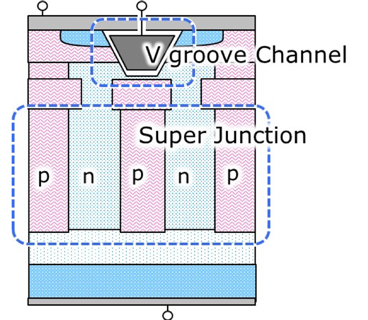
We have developed "V-groove type metal-oxide-semiconductor structure transistor (VMOSFET)" using silicon carbide (SiC) until now. By utilizing a variety of crystal plane orientations, an oxide film interface with few defects is formed and realize a power transistor that achieves both low on-resistance and high withstand voltage.
A VMOSFET is a device that has a low on-resistance by applying a unique channel structure to the channel section above the device that controls the on / off of current.
We have newly applied a super junction structure to the breakdown voltage holding layer (drift layer) (Figure). The super junction structure has been proven to be effective in reducing the resistance of silicon transistors and has been put to practical use. However, the application method for SiC had a problem with the manufacturing method, and remained at the proof-of-principle level.
Through joint development with National Institute of Advanced Industrial Science and Technology and so on, we have overcome the conventional problems and realized the SiC super junction structure by forming a narrow pitch p-type and n-type columnar structure by repeating epitaxial growth and ion implantation. Achieving a low on-resistance of 1,170 V / 0.63 mΩcm2 by applying a design and process that matches the low-channel-resistance VMOSFET structure has already been reported at conferences.
For practical realization, it is necessary to create devices with the above-mentioned complicated structure at low cost, and we are developing new technologies for that purpose. By 2030, we will realize a low on-resistance device with a withstand voltage of 1,200 V and less than 1.0 mΩcm2, contributing to energy saving and CO2 reduction.
Supplementary information
Other Innovation Challenges
Development and Dissemination of High-Temperature Superconducting Technology
Sumitomo Electric Industries, Ltd.
Increase power generation efficiency using concentrator photovoltaic System (CPV)
Sumitomo Electric Industries, Ltd.
Similar Innovation Challenges
Achieve 2050 decarbonization target with Net Zero Energy House!
Sekisui House, Ltd.
Achieving net-zero emissions by promoting renewable energy use through both our monozukuri and products.
DAIWA HOUSE INDUSTRY CO., LTD.

